Skip links

iWave iW-RainboW-G24M Arria 10 FPGA SOM

iWave iW-RainboW-G24M Arria 10 FPGA SOM

iWave iW-RainboW-G24M Arria 10 FPGA SOM

  • Arria 10 FPGA device compatibility (GX270, GX320, GX480, GX570, GX660, GX900, GX1150)
  • With upto 1150K Logic Elements and 24 High Speed transceivers
  • 4-GB DDR4 RAM (64bit) & 2-GB DDR4 RAM for FPGA
  • 24 high-speed transceivers @ 17.4Gbps
  • 48/96 LVDS from BANK 3B & 3C and 93 SE from BANK 2A & 3A
  • Dual 240 Pin Board to Board Connector
  • Variable IO voltage support from PMIC
  • Industrial Grade operation
  • 10+ Years Longevity

SKU: iWave iW-RainboW-G24M Arria 10 FPGA SOM

Description

Karta katalogowa Manual

On Module Feature:

  • Compatible Arria10 FPGA Family – GX270, GX320, GX480, GX570, GX660, GX900, GX1150
    • Up to 1150K Logic elements
    • High Speed Transceivers x 24 @ 17.4 Gbps
  • 2-GB DDR4 RAM (32bit) from FPGA
  • 4-GB DDR4 RAM (64bit) from FPGA (only in GX480 or higher family devices)
  • Configuration Flash for FPGA
  • Other On SOM features
    • JTAG Header
    • 5V-FAN Header
    • FPGA AS Header
    • FPGA Configuration Selection Switch

Two 240pin High Speed Board to Board Connectors Interfaces

From connector 1 interface
  • FPGA High Speed Transceivers (upto 17.4Gbps) x 16
  • FPGA IOs & General Purpose Clocks – Bank2A
    • Up to 21 LVDS/46SE IOs
    • One General Purpose Clock Input LVDS Pair/Single Ended
    • Two General Purpose Clock Output LVDS Pairs/Single Ended
  • FPGA IOs & General Purpose Clocks – Bank3A
    • Up to 22 LVDS/47SE IOs
    • Two General Purpose Clock Input LVDS Pairs/Single Ended
    • Two General Purpose Clock Output LVDS Pairs/Single Ended
From connector 2 interface
  • Gigabit Ethernet x 1 Port (through On-SOM Gigabit Ethernet PHY from Bank2L IOs)
  • USB OTG x 1 Port (through On-SOM USB ULPI PHY from Bank2L IOs)
  • Upto 20 Single-Ended IOs
  • FPGA AS Interface (Optional)
  • FPGA High-Speed Transceivers (up to 17.4Gbps) x 8
  • FPGA IOs & General Purpose Clocks – Bank3B
    • Up to 24 LVDS IOs/48SE IOs
    • Two General Purpose Clock Input LVDS Pairs/Single Ended
    • Two General Purpose Clock Output LVDS Pairs/Single Ended
  • FPGA IOs & General Purpose Clocks – Bank3C
    • Up to 24 LVDS IOs/48SE IOs
    • Two General Purpose Clock Input LVDS Pairs/Single Ended
    • Two General Purpose Clock Output LVDS Pairs/Single Ended
  • JTAG Interface

General Features:

Power Input 5V
Operating Temperature -40°C to +85°C
Form Factor 75mm x 95mm
BSP Support Linux BSP:- Linux 5.4/Quartus 21.3
Environment Specification RoHS &REACH Compliant
Compliance CE*

DEVELOPMENT KIT

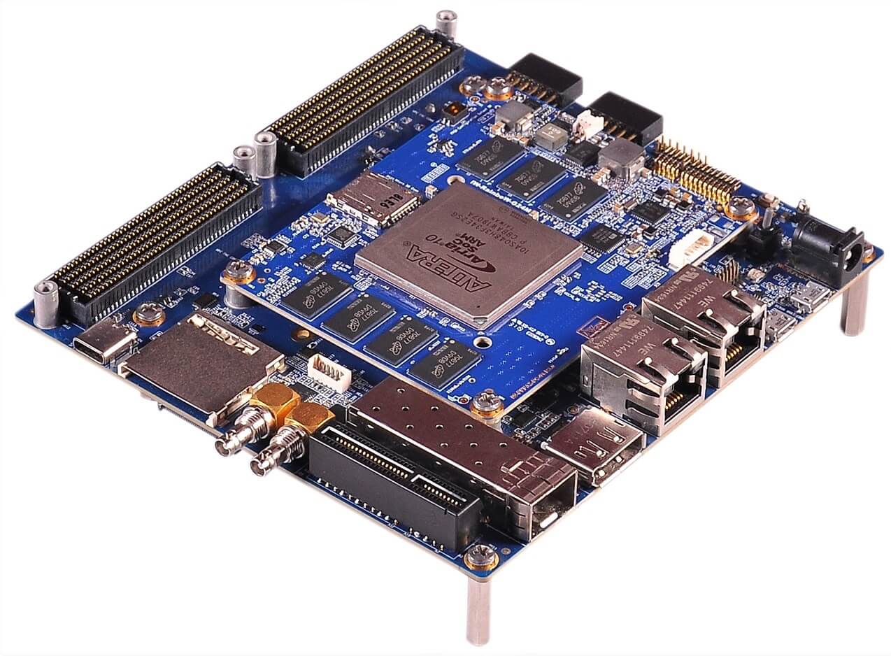
  • Gigabit Ethernet through RJ45MagJack x 1
  • USB2.0 OTG through Micro AB connector x 1
  • Debug UART through USB Micro AB connector x 1
  • 10G Ethernet through SFP+ Connector
  • PCIe Gen3 x 1 Connector
  • Dual PMOD Connector
  • Dual FMC High Pin Count (HPC) Connector
  • SDI Video IN through HD BNC Connector x 1
  • SDI Video Out through HD BNC Connector x 1
  • M.2 SATA Connector x 1
  • USB3.0 TypeC connector x 1
  • Display Port Connector x 1
  • Clock Synthesizer/Generator
  • 16-Bit IO Expander
    JTAG Connector x 1
    20 Pin GPIO Header x 1
  • RTC Coin Cell Holder
    Power ON/OFF DIP Switch x 1
  • Reset Push button Switch x 1
  • Power Supply : DC 12V, 5A Power Input Jack
  • Form Factor: 130mm x 140mm
Zainteresowany tym produktem?

Serdecznie zapraszamy do kontaktu!


    Szanujemy Twoją prywatność, nie tolerujemy spamu i nigdy nie sprzedajemy, nie udostępniamy Twoich danych!


    Wyrażam zgodę na przetwarzanie moich danych i akceptuję Politykę prywatności